
NVIDIA Blackwell's Memory Architecture: A Generational Leap for AI
As AI models continue their exponential growth, memory capacity, bandwidth, and latency consistently present the most formidable challenges for hardware engineers. The need for larger models often forces developers into

As AI models continue their exponential growth, memory capacity, bandwidth, and latency consistently present the most formidable challenges for hardware engineers. The need for larger models often forces developers into complex multi-GPU setups, aggressive quantization, or undesirable performance trade-offs. NVIDIA's Blackwell architecture, the successor to Hopper, directly confronts this problem by fundamentally re-engineering how memory is structured and accessed at the hardware level.
This article delves into the significant memory enhancements that position Blackwell as a groundbreaking AI accelerator, enabling tasks like running large language models such as Llama 3 70B without the previous limitations of parallelization or tight memory constraints.
Blackwell's Generational Memory Overhaul
The shift from Hopper to Blackwell represents a profound evolution in GPU memory design. Let's look at the key changes:
| Spec | Hopper H100 | Blackwell B200 | Change |
|---|---|---|---|
| HBM Capacity | 80 GB (HBM3) | 192 GB (HBM3e) | 2.4× |
| HBM Bandwidth | 3.35 TB/s | 8 TB/s | 2.4× |
| L2 Cache | 50 MB | 126 MB | 2.5× |
| L1/Shared per SM | 256 KB | 128 KB | 0.5× |
| Die Design | Monolithic | Dual-die (MCM) | — |
| CPU Integration | Separate (PCIe) | Unified (NVLink C2C) | — |
The numbers clearly indicate a substantial increase in memory capacity, bandwidth, and cache size, alongside fundamental changes in die design and CPU integration. These are the pillars of Blackwell's advanced memory architecture.
The GB200 Superchip: A Unified Computing System
The Grace Blackwell (GB200) superchip extends NVIDIA's unified computing vision, pairing an ARM-based Grace CPU with two Blackwell GPUs. This integration is facilitated by NVLink Chip-to-Chip (NVLink-C2C), creating a single, cohesive system where the CPU and GPUs can share memory.
Grace CPU and LPDDR5X: Extended GPU Memory (EGM)
The Grace CPU, an ARM Neoverse V2 processor, is engineered for high bandwidth and efficiency. It manages general-purpose tasks, data pre-processing, and tokenization, efficiently feeding data to the GPUs via NVLink C-2-C. Crucially, the Grace CPU effectively acts as an extended memory tier for the GPUs, leveraging its dedicated LPDDR5X memory.
LPDDR5X is a high-speed, power-efficient memory standard, delivering up to 500 GB/s bandwidth with low power consumption (around 16W). It includes approximately 100MB of L3 Cache. When accessed from the GPU via NVLink C-2-C, the bandwidth can reach ~900 GB/s, making it a critical high-speed overflow tier for data that doesn't fit into the GPU's HBM.
Blackwell GPU: Dual-Die Innovation
Blackwell GPUs introduce a dual-die Multi-Chip Module (MCM) design, with two individual GPU dies housed within a single module. Each die contains 104 billion transistors, summing to 208 billion for the complete GPU. The dies are connected by a rapid 10 TB/s NVIDIA High-Bandwidth Interface (NV-HBI), ensuring they operate as a unified GPU.
Each die contributes 96 GB of HBM3e memory, resulting in 192 GB total per GPU. Of this, 180 GB is usable, with the remainder reserved for ECC, system firmware, and overhead. This configuration boosts HBM bandwidth to 8 TB/s, a 2.4x improvement over Hopper's HBM3. Furthermore, the L2 cache has been significantly expanded to 126 MB, a 2.5x increase, allowing Blackwell to retain more model weights and intermediate results on-chip, thereby reducing trips to the slower HBM and keeping compute units fed.
NVLink C-2-C: Coherent Memory Across Chips
The NVLink C-2-C interconnect provides a ~900 GB/s communication link between the Grace CPU and the Blackwell GPUs. This far surpasses the typical PCIe Gen6 speed of ~128 GB/s. More importantly, NVLink C-2-C ensures cache coherence, allowing the CPU and GPU to share a unified memory architecture, often referred to as Unified CPU-GPU Memory or Extended GPU Memory (EGM).
Blackwell's Layered Memory Hierarchy
Understanding data flow within Blackwell's memory hierarchy is essential for optimizing AI workloads. Data moves through progressively larger but slower memory tiers as it moves further from the compute units.
| Memory Tier | Capacity | Bandwidth | Purpose |
|---|---|---|---|
| Registers | ~256 KB per SM | Immediate | Active computation |
| L1/Shared Memory | ~128 KB per SM | ~40 TB/s aggregate | Data staging, inter-thread sharing |
| L2 Cache | ~126 MB total | ~20 TB/s | Cross-SM data reuse |
| HBM3e | 192 GB (180 usable) | 8 TB/s | Model weights, activations |
| LPDDR5X (CPU) | ~480 GB | ~900 GB/s (from GPU) | Overflow, large embeddings |
On-Chip Memory: Registers, L1/Shared, and L2 Cache
Each Streaming Multiprocessor (SM) has registers for active computations and configurable L1/Shared memory. Blackwell's L1/Shared memory is 128 KB per SM, a reduction from Hopper's 256 KB. This design choice was made to allocate more capacity to TMEM for Tensor Core operations, with a larger L2 cache compensating for general-purpose workloads. The aggregate L1/Shared bandwidth across all SMs is approximately 40 TB/s.
The L2 cache, shared across all compute units on a die, is now 63 MB per die, totaling 126 MB for the B200 GPU. This substantial increase is critical for AI inference, where repeated access to model weights benefits significantly from on-chip caching, reducing latency and boosting throughput. The dual-die design means L2 access across dies, though still fast via NV-HBI, is slower than local L2 access.
Main Memory Pool: HBM3e
HBM3e serves as the primary storage for large model components like weights, activations, and input data. Blackwell features 192 GB of HBM3e (180 GB usable), delivering an impressive 8 TB/s of bandwidth. This ensures that the hungry Tensor Cores receive data fast enough to prevent stalls and maximize utilization during intensive matrix multiplications.
Extended Tier: LPDDR5X
Beyond the GPU's HBM lies the Grace CPU's LPDDR5X memory, offering approximately 480 GB of additional, high-speed storage. While its bandwidth (when accessed from the GPU) is about 10x lower than HBM, it is significantly faster than traditional storage. LPDDR5X functions as a crucial overflow tier for vast datasets that exceed HBM capacity, such as large embedding tables, KV caches for long-context inference, or checkpoint buffers, mitigating severe performance penalties.
Practical Impact: Running Llama 3 70B
Consider running Llama 3 70B for inference. In FP16 precision, this model requires about 140 GB of memory for its weights alone.
- On a Hopper H100 (80 GB HBM3): The model cannot fit. Developers would need aggressive quantization, tensor parallelism across multiple GPUs, or slow offloading to CPU memory via PCIe.
- On a single GB200 Superchip (~360 GB usable HBM3e + ~480 GB LPDDR5X): The entire 140 GB model fits comfortably within one GPU's HBM. The remaining GPU's HBM and the vast CPU memory pool are available for KV caches, larger batch sizes, or even running multiple model instances. This eliminates the need for complex model parallelism or forced quantization due to memory limitations. A single GB200 Superchip offers roughly 10x the usable memory of a single H100.
This dramatic increase in available and accessible memory fundamentally simplifies AI deployment and boosts efficiency by reducing inter-GPU communication overhead.
Conclusion
Blackwell's memory architecture marks a pivotal moment in AI hardware. By integrating dual-die GPUs with high-bandwidth HBM3e and establishing unified CPU-GPU memory via NVLink C-2-C, NVIDIA has delivered a system that significantly alleviates memory constraints. AI engineers can now focus more on model innovation and less on architectural workarounds, leveraging systems that are not only faster but also inherently simpler to program and deploy. This memory-first approach positions Blackwell as a blueprint for future GPU architectures, emphasizing tighter integration and unified memory pools to tackle the ever-growing demands of AI.
FAQ
Q: Why did NVIDIA reduce the L1/Shared memory per SM in Blackwell compared to Hopper?
A: NVIDIA reduced the L1/Shared memory per SM from 256 KB in Hopper to 128 KB in Blackwell primarily to shift capacity towards TMEM (Tensor Memory) for more efficient Tensor Core operations. This was compensated by a significant increase in the shared L2 cache size (from 50 MB to 126 MB), which is more effective for data reuse across SMs and batches in AI workloads.
Q: How does the Grace CPU's LPDDR5X memory contribute to the Blackwell GPU's performance?
A: The Grace CPU's LPDDR5X memory serves as a high-speed extended memory tier for the Blackwell GPUs. Connected via NVLink C-2-C at ~900 GB/s, it allows data that exceeds the GPU's HBM capacity (such as very large embedding tables or long-context KV caches) to reside in CPU memory without incurring catastrophic performance penalties typical of PCIe or disk access. This greatly expands the effective usable memory footprint of the GB200 superchip.
Q: What is the significance of Blackwell's dual-die (MCM) design and the NV-HBI?
A: Blackwell's dual-die Multi-Chip Module (MCM) design allows NVIDIA to integrate two large GPU dies into a single package, effectively doubling the compute resources and memory capacity that would be difficult to achieve with a single monolithic die. The NVIDIA High-Bandwidth Interface (NV-HBI) provides a blazing 10 TB/s connection between these two dies, enabling them to communicate and function as a single, unified GPU, sharing resources and presenting a cohesive programming model.
Related articles

Sakana AI Launches 'Ultra Deep Research' Agent: 100+ Page Reports in
Sakana AI has launched Marlin, an "ultra deep research" agent designed for enterprise clients. Operating as a "Virtual CSO," Marlin conducts self-governing reasoning for up to eight hours to deliver comprehensive, 100+ page strategy reports. Powered by Adaptive Branching Monte Carlo Tree Search (AB-MCTS) and a multi-LLM architecture, it focuses on deep, vetted analysis over quick generation, backed by strict data privacy policies and significant venture capital.
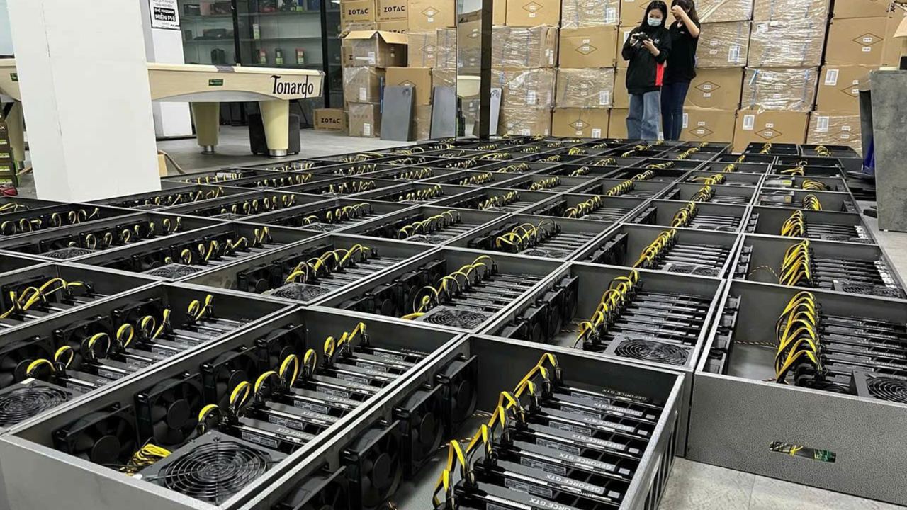
Pearl AI Cryptomining: Empty Promises, Real Costs
Pearl, a Layer-1 blockchain, claims to merge crypto mining with useful AI computation, but new research suggests its 320,000-GPU network burns 112MW on "zero useful AI computation," driving up GPU rental prices.
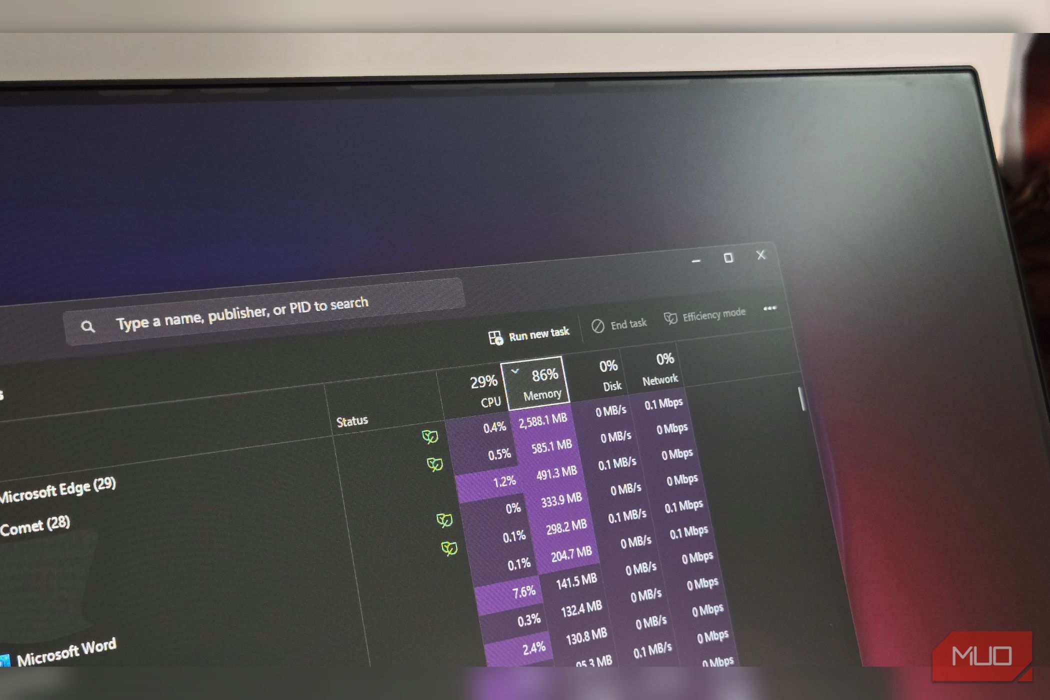
Why Disabling Windows Prefetch Makes Your PC Slower and How to
Discover why turning off Windows Prefetch can degrade performance, understand how Windows manages memory efficiently, and learn to correctly interpret your PC's RAM usage in Task Manager.

Kickstart Your Tech Career with freeCodeCamp: A Deep Dive
The technology landscape is in a constant state of flux, rapidly reshaping industries and creating new opportunities. For many aspiring developers, navigating this dynamic environment and identifying a clear path to
Engineering Leadership in the Era of Near-Zero Code Cost
AI is pushing the cost of code generation to near zero, profoundly reshaping engineering leadership. This shift moves the bottleneck from coding speed to ideation and process, necessitating a re-evaluation of how teams measure effectiveness and collaborate. Engineering leaders must now prioritize customer value, foster cross-functional empathy, and emphasize system ownership over raw code output.
GeoLibre 1.0: Cloud-Native GIS for the Modern Developer Stack — Key
For too long, geospatial data visualization and analysis have been associated with heavy desktop applications and intricate server setups. While powerful, traditional GIS tools often present steep learning curves,