
Lace Secures $40M to Revolutionize Chip-Making with Helium Atoms
Norwegian startup Lace has secured $40 million in Series A funding to advance its groundbreaking chip-making technology. The company plans to replace traditional light-based lithography with helium atom beams, promising chip features up to ten times smaller than current capabilities. This investment, led by Atomico and including Microsoft's M12, highlights a strategic push to diversify the semiconductor supply chain and meet growing AI demand.
In a significant move poised to disrupt the semiconductor industry, Norwegian startup Lace has announced a successful $40 million Series A funding round. The Bergen-based company is developing a groundbreaking lithography technology that employs helium atoms instead of light to etch chip patterns, promising features up to ten times smaller than current industry standards.
The Series A investment was led by European venture capital firm Atomico, with notable participation from Microsoft’s venture arm M12, Linse Capital, Norwegian state climate investment company Nysnø, and the Spanish Society for Technological Transformation. This substantial backing underscores the strategic importance and potential of Lace’s innovative approach to chip manufacturing.
Challenging the Lithography Landscape
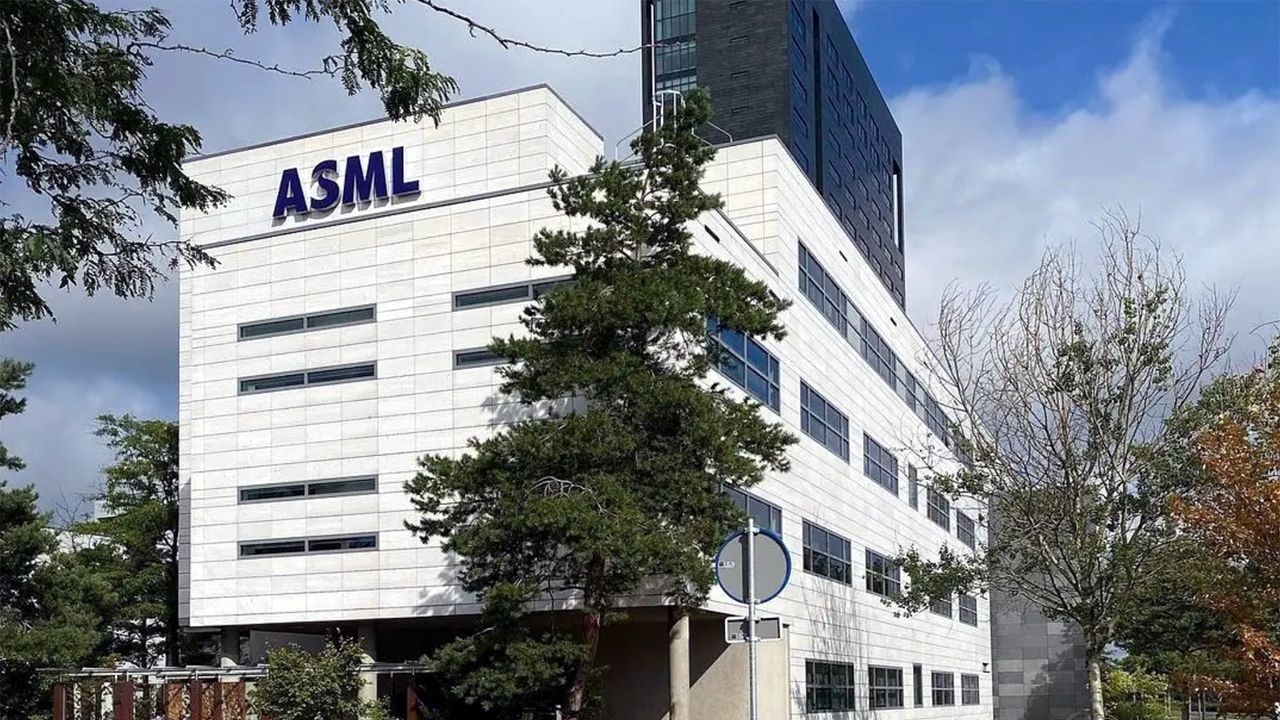
The global semiconductor industry heavily relies on extreme ultraviolet (EUV) lithography systems, predominantly manufactured by Dutch giant ASML. These highly advanced machines, costing upwards of $350 million each, utilize light with a 13.5 nanometer wavelength to define chip circuits, forming the bedrock of modern AI hardware. ASML currently holds a near-monopoly on these critical systems.
Lace aims to introduce a credible alternative. Founded in July 2023 by physicist Bodil Holst and her former PhD student Adria Salvador Palau, the company’s technology harnesses a beam of helium atoms. This atomic beam is approximately 0.1 nanometers wide—roughly the size of a single hydrogen atom—making it about 135 times finer than ASML’s EUV light. If successfully scaled for manufacturing, this could enable transistors and other structures at what Holst terms “ultimately atomic resolution.”
Scientific Foundations and Future Outlook
Bodil Holst, a Danish-Norwegian physicist who joined the University of Bergen in 2007, built her research career on nanoscale imaging, molecular-beam lithography, and 2D materials. She continues to hold an affiliated professorship at the university while serving as Lace's CEO. CTO Adria Salvador Palau completed his PhD under Holst at Bergen and now operates from Barcelona.
Prior to its Series A, Lace received pre-seed investments from the European Innovation Council and Innovasjon Norge, Norway’s national innovation agency. The company has already developed prototype systems and publicly shared its research findings at a scientific lithography summit in February 2026. Looking ahead, Lace targets the deployment of a test tool in a pilot chip fabrication plant around 2029, marking a crucial step towards commercialization.
Geopolitical and Strategic Significance
Lace’s emergence comes at a time when governments and investors are prioritizing diversification in the semiconductor supply chain. This push is driven by increasing geopolitical tensions, particularly concerning export controls on advanced lithography equipment to China, and the burgeoning demand for chips fueled by artificial intelligence advancements.
ASML's dominant position, while technically impressive, has become a politically sensitive flashpoint in the broader technological competition between global powers. A viable alternative to EUV, even one a decade away from full commercial deployment, holds substantial strategic value. The diverse investor syndicate, including a European VC, a Norwegian state fund, and a Spanish government-affiliated investor, suggests that Lace is being supported as much for its geopolitical optionality as for its long-term commercial potential, aiming to introduce competition and resilience into the global chip ecosystem.
FAQ
Q: What is Lace's core technology for chip manufacturing?
A: Lace's core technology involves using a beam of helium atoms, rather than light, to etch patterns onto chips, enabling significantly smaller and more precise features.
Q: How much finer can Lace's technology make chip features compared to current methods?
A: Lace's technology is designed to create chip features up to ten times smaller than what current extreme ultraviolet (EUV) lithography systems can achieve.
Q: Who were the key investors in Lace's $40 million Series A funding round?
A: The Series A round was led by Atomico, with participation from Microsoft’s M12, Linse Capital, Nysnø (a Norwegian state climate investment company), and the Spanish Society for Technological Transformation.
Related articles

Pentagon Halts 155 Wind Projects in 24 States Over Drone Fears
The Pentagon has frozen permitting for 155 wind projects across 24 states for nearly a year, citing concerns that drones can hide within wind farms. This impacts 44 gigawatts of capacity and has cost developers $2 billion. The wind industry claims the freeze is politically motivated and has filed a lawsuit.

Build Your Own Local NMT App with React Native and QVAC
This article explores how Neural Machine Translation (NMT), powered by the Transformer architecture, revolutionized translation by understanding context. We then delve into QVAC, a local-first AI development platform, and its Bergamot engine, enabling private, on-device translation. Learn to set up a React Native app with QVAC and manage model lifecycles for efficient local translation.
ASML Low-NA EUV Pricing: Value Capture or Cost Burden
The Industry Reacts: ASML's EUV Pricing Shift Verdict: ASML’s strategic move to broaden its value-based pricing for Low-NA EUV tools, looking beyond mere wafer throughput, marks a significant shift in the semiconductor
in-depth: Chewy Promo Codes: $20 Off July 2026: coupons — Key Details
Pet owners can find substantial savings at Chewy in July 2026. New customers get $20 off first orders (code WELCOME) and free shipping. Existing users benefit from exclusive deals, Autoship discounts, and a Chewy+ membership for ongoing perks and rewards.

Kalshi says it caught Trump’s teleprompter operator insider trading
Prediction market platform Kalshi has accused Donald Trump's teleprompter operator, Gabriel Perez, of insider trading, alleging he used advance knowledge of Trump's speeches to win over $100,000. Kalshi flagged the activity and referred it to the CFTC. While federal prosecutors declined a criminal case, a settlement is being discussed.

AI-powered travel agency Fora hits unicorn status, raises $60M
Fora, the innovative AI-powered travel agency, has officially joined the ranks of billion-dollar companies, announcing a $60 million Series D funding round that solidifies its unicorn status. The capital injection, led