
Prinano Photonic Chip Production: Promising Potential, Key Questions
Verdict: A Glimmer of Hope with Caveats Chinese startup Prinano has made a significant claim: successfully validating the mass production of photonic chips using an innovative nanoimprint lithography (NIL) process,
Verdict: A Glimmer of Hope with Caveats
Chinese startup Prinano has made a significant claim: successfully validating the mass production of photonic chips using an innovative nanoimprint lithography (NIL) process, completely sidestepping traditional deep-ultraviolet (DUV) lithography. This development, if substantiated with comprehensive data, could be a game-changer for China's semiconductor independence and for the photonics industry globally, promising a drastic 90% cost reduction. However, while the technical feasibility on 8-inch wafers for photonic chips is compelling, the absence of crucial commercial metrics like yield rates, defect densities, or independent validation means this announcement, for now, represents a promising technological advancement rather than a proven commercial breakthrough. It’s a bold step forward in an alternative manufacturing pathway, but the journey to widespread adoption is still unclear.
Unpacking the Technology: Nanoimprint vs. Traditional Lithography
Modern semiconductor manufacturing largely relies on highly advanced optical lithography systems, specifically DUV and the even more cutting-edge extreme ultraviolet (EUV) systems. These machines, produced by companies like ASML, project intricate circuit patterns onto silicon wafers using light, involving some of the most complex optics ever engineered, often costing hundreds of millions of dollars. For China, access to these critical DUV and EUV tools has been severely restricted by export controls, pushing domestic companies to seek alternative manufacturing routes.
Prinano's proposed solution, its PL-AS vacuum air-cushion nanoimprint lithography (NIL) system, takes a fundamentally different approach. Instead of light projection, NIL physically stamps microscopic patterns directly onto a specially prepared resist layer on the wafer surface. This process inherently eliminates the need for many of the expensive optical systems found in conventional lithography, which is the basis for Prinano's claim of a roughly 90% reduction in manufacturing costs compared to DUV-based processes.
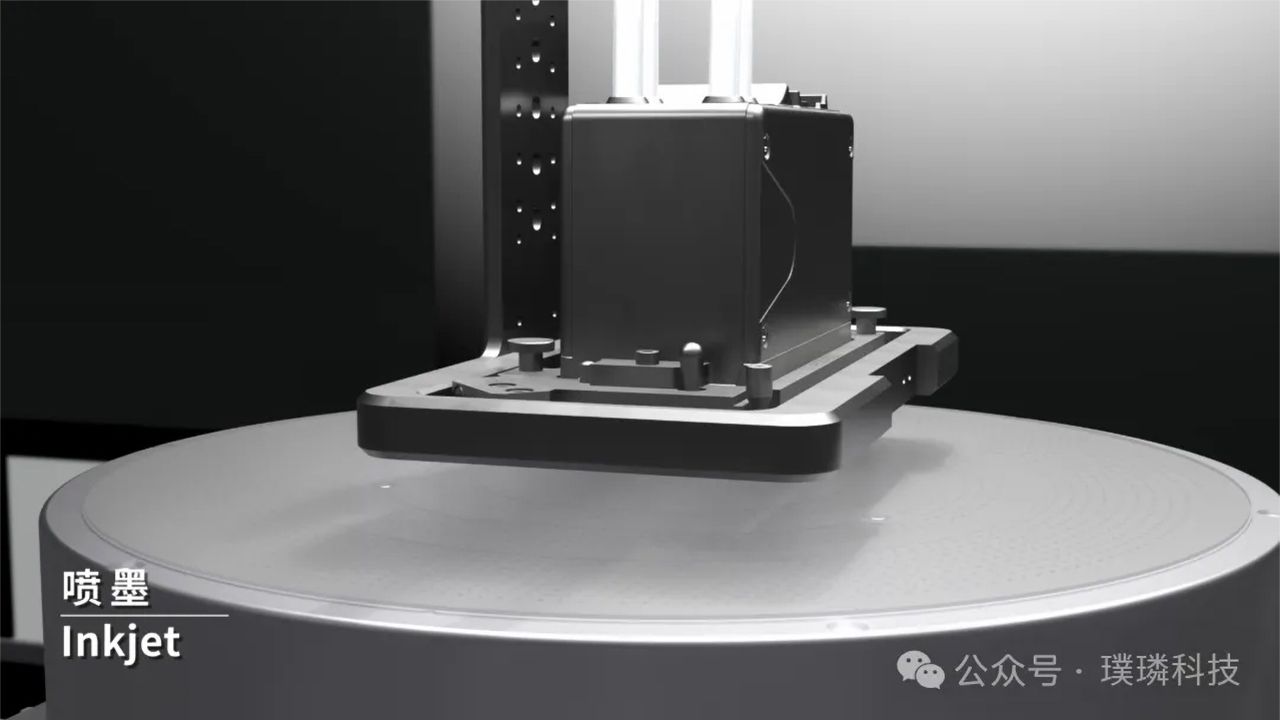
Key Details and Prinano's Claims
Prinano, established in 2017, has been dedicated to overcoming the historical hurdles of NIL. Their latest announcement, made via a WeChat post following an SCMP report, indicates they've moved beyond pilot deployments. In collaboration with Shenzhen Litra Technology, Prinano claims to have produced 8-inch optical chip wafers using their proprietary NIL platform. This platform reportedly integrates wafer-level pressure control, bespoke double-layer imprinting materials, and proprietary process technologies, enabling the production of sub-10-nanometer features.
Crucially, Prinano is not aiming to replace the production of advanced logic processors or AI accelerators, which are extremely sensitive to defect rates and alignment. Instead, their focus is on photonic chips – semiconductors that manipulate light signals rather than electrical ones. These chips are vital for fiber-optic communications, data centers, sensing systems, and LiDAR technologies. Photonic chips are particularly well-suited for NIL because their critical structures, such as waveguides and gratings, often consist of repeating nanoscale patterns that can be efficiently replicated through stamping techniques.
The use of 8-inch wafers is another noteworthy detail. While leading-edge processors have migrated to larger 12-inch wafers, 8-inch wafers remain a staple in specialized sectors, including compound semiconductors and power electronics. Demonstrating production on full 8-inch wafers suggests that Prinano's process has matured beyond mere laboratory experiments and can operate in a format compatible with commercial manufacturing.
A Closer Look: Nanoimprint vs. DUV/EUV
Here's a breakdown of how nanoimprint lithography, as presented by Prinano, stacks up against traditional methods:
| Feature | Traditional DUV/EUV Lithography | Nanoimprint Lithography (NIL) - Prinano's Approach |
|---|---|---|
| Mechanism | Projects patterns using light onto resist | Physically presses nanoscale patterns into resist |
| Equipment Cost | Hundreds of millions of dollars (high) | Significantly lower (claims 90% reduction) |
| Complexity | Highly sophisticated optical systems | Eliminates many expensive optical systems |
| Resolution | Extremely high, leading-edge (EUV: sub-10nm) | Claims sub-10nm features |
| Primary Use | Modern logic chips, CPUs, AI accelerators | Photonic chips (waveguides, gratings) |
| Challenges (Historical) | High cost, export restrictions for China | Defect rates, template wear, throughput, yield |
| Prinano's Claimed Progress | N/A | Overcomes historical NIL limitations |
| China Dependence | High (on ASML equipment) | Greatly reduced/eliminated (domestic tech) |
The Honest Truth: Pros and Cons
Pros:
- Cost Reduction: The most significant potential advantage is the claimed 90% reduction in manufacturing costs compared to DUV. This could democratize photonic chip production and open new markets.
- Independence from DUV/EUV: For China, this technology offers a critical pathway to reduce reliance on restricted ASML lithography tools, aligning with national strategic goals.
- Suitability for Photonic Chips: NIL's ability to efficiently replicate repeating nanoscale patterns makes it an ideal fit for photonic chip structures like waveguides and gratings.
- Sub-10nm Feature Capability: Prinano's claim of achieving sub-10nm features suggests high precision, competitive with advanced lithography nodes.
- 8-inch Wafer Validation: Moving beyond lab-scale into 8-inch wafer production is a strong indicator of commercial readiness and scalability.
Cons:
- Lack of Commercial Metrics: The biggest question mark is the absence of crucial data. Prinano has not disclosed production volumes, yield rates, defect densities, customer shipment details, or any independent third-party validation. These metrics are fundamental to proving commercial viability, not just technical feasibility.
- Historical NIL Challenges: Nanoimprint lithography has historically struggled with defect rates, template wear, throughput, and overall production yields in high-volume manufacturing environments. While Prinano claims to have overcome these, concrete proof is still missing.
- Limited Application Scope: While excellent for photonic chips, NIL, in its current claimed form, is not positioned as a direct replacement for producing cutting-edge logic chips, which require extremely tight alignment and minimal defects across a vast number of transistors.
The Bigger Picture: China's Tech Ambitions
Prinano's announcement is a microcosm of China's broader strategy to navigate ongoing export restrictions. Faced with limited access to advanced lithography equipment, Chinese companies are aggressively pursuing alternative paths, from advanced packaging to novel chip architectures (like Huawei's LogicFolding) and innovative manufacturing methods. Prinano's success with NIL for photonics could pave the way for other specialized chip types, diversifying China's domestic semiconductor capabilities.
Recommendation: Proceed with Cautious Optimism
For industries heavily reliant on photonic chips – telecommunications, data centers, autonomous vehicles (LiDAR) – Prinano's nanoimprint lithography presents a highly intriguing prospect. The potential for massive cost reductions and a diversified supply chain is undeniably attractive. However, any serious consideration, whether for partnerships, investment, or adoption, must await the disclosure of robust, independently verified commercial performance data. Technical validation is one thing; sustained, high-volume commercial production with acceptable yields and defect rates is another entirely. Prinano has demonstrated technical progress, but the commercial proof is still outstanding. We remain cautiously optimistic, eager for more transparency and concrete results.
FAQ
Q: Is Prinano's technology a direct replacement for ASML's DUV/EUV machines for all types of chips?
A: No, Prinano's announcement specifically focuses on photonic chips, which manipulate light. While promising for this specialized category, it is not positioned to replace DUV or EUV for the production of advanced logic processors (CPUs, AI accelerators) where different requirements for defect rates and alignment apply.
Q: What are the biggest hurdles Prinano still needs to overcome to prove commercial viability?
A: The main hurdles are the lack of disclosed commercial metrics. Prinano needs to provide transparent data on actual production volumes, yield rates, defect densities, and independent third-party validation to demonstrate that its technology is not just technically feasible but also commercially viable for high-volume manufacturing.
Q: How does Prinano's claimed 90% cost reduction impact the industry?
A: If validated, a 90% cost reduction for photonic chip manufacturing could significantly lower the barrier to entry for many applications, potentially leading to cheaper fiber optics, more affordable LiDAR sensors, and more cost-effective data center interconnects. This could accelerate innovation and deployment of photonics technologies globally, assuming the quality and reliability are on par with existing methods.
Related articles

Seattle's AI 911 Routing: Critical Failure in Transparency
Quick Verdict Seattle's implementation of an AI system to triage and route 911 medical calls, developed by Denmark-based Corti, is a deeply problematic deployment of technology in a critical public safety service.

Netflix's Lincoln Lawyer Ending: A Satisfying Farewell
The Lincoln Lawyer Cancellation: Not So Bad After All Verdict: While Netflix's decision to end The Lincoln Lawyer with its fifth season might initially sound like another disappointing cancellation, the situation is

Google Messages Optimization: Essential Settings for a Better
A comprehensive review of ZDNET's recommended 9 Google Messages settings for enhanced privacy, reduced clutter, and a tailored user experience on Android devices, offering a pragmatic guide to optimize your messaging.

Computex 2026: A Practical Turn for PC Hardware
Computex 2026: Practicality Over Brute Force Verdict: Computex 2026 wasn't about flashy spec bumps, but a refreshing shift towards practicality, user experience, and accessibility. The PC industry is finally maturing,

Ars Technica Article: Medieval Comet Mystery - An Engaging Historical
Verdict: A Captivating Look into Medieval Science and Legend Ars Technica's piece, "Did a medieval flying monk spot Halley’s comet, twice? It’s complicated," delivers a fascinating exploration of a niche historical

GeekWire's Weekly Roundup: A Concise Pulse on Pacific Northwest Tech
Verdict GeekWire's "Week in Review" for June 7, 2026, serves as a highly effective, albeit somewhat cluttered, digest for anyone keen on the technology landscape, particularly within the Pacific Northwest. It offers a