
Terafab EUV Tool: Ambitious but Delayed Vision
Quick Verdict Elon Musk's Terafab, an ambitious venture into advanced semiconductor manufacturing, is reportedly set to receive its first cutting-edge Extreme Ultraviolet (EUV) lithography tool from ASML in mid-2027.
Quick Verdict
Elon Musk's Terafab, an ambitious venture into advanced semiconductor manufacturing, is reportedly set to receive its first cutting-edge Extreme Ultraviolet (EUV) lithography tool from ASML in mid-2027. While this signifies a major step towards realizing the internal chip production goals for Tesla, SpaceX, and xAI, the timeline suggests this multi-million dollar piece of equipment could sit idle for a significant period. The facility's experimental development fab is projected to see its shell completed by late 2027, with equipment installation extending well into 2028, leading to actual wafer processing only by early 2029. This strategic move leverages Intel's 14A process technology, signaling a pragmatic approach over experimental light sources, albeit positioning Terafab slightly behind the absolute leading edge of foundry technology upon its full volume ramp in mid-2030.
The Vision: What is Terafab?
Terafab represents Elon Musk's foray into in-house semiconductor manufacturing, a critical move designed to secure chip supply for his various ventures: Tesla (electric vehicles, AI), SpaceX (aerospace, Starlink), and xAI (artificial intelligence). Announced with significant scale—rumored to encompass 100 million square feet of manufacturing space and an initial investment of $16.8 billion—Terafab aims to bring advanced chip production under direct control, minimizing reliance on external foundries and potentially optimizing designs for specific applications across these diverse companies. This horizontal integration strategy is a bold departure from the typical fabless or IDM models in the industry.
Key Details: The ASML EUV Acquisition
At the heart of advanced chipmaking lies Extreme Ultraviolet (EUV) lithography, a technology exclusively supplied by Dutch giant ASML. Terafab is slated to receive its first ASML Twinscan NXE EUV lithography tool in mid-2027. This is a conventional EUV system, despite Musk's past expressions of interest in more experimental Free Electron Laser (FEL) light sources. This choice is practical, as conventional EUV is a proven technology essential for nodes like Intel's 14A (1.4nm-class), which Terafab is adopting. The scanner is a cornerstone for producing the intricate patterns required for next-generation chips, utilizing both existing Low-NA and future High-NA EUV capabilities required for the 14A node.
The Build-Out and Timeline Challenges
Groundbreaking for Terafab's research fab at Giga Texas occurred in April 2027. Initial construction, as observed from drone footage in mid-September, showed foundational work underway. However, the timeline for operational readiness stretches well beyond the EUV tool's mid-2027 arrival. The development fab's shell is anticipated to be complete by late 2027, with equipment installation reportedly taking another six months after the main building is finished (projected July 2028). This means the multi-million-dollar EUV machine could sit idle for over a year before it begins processing its first experimental wafers, estimated for early 2029.
The volume production facility, Terafab Grimes Phase 1, has an even longer gestation period. Analysts project a 20-month construction phase, 17 months for equipment outfitting, and a 6-month ramp to volume. This places its full operational start in late 2029, with high-volume manufacturing (HVM) targeted for mid-2030. Interestingly, SpaceX reportedly ordered manufacturing equipment as early as April 2026, months before the Grimes County location was even officially announced, highlighting their early commitment and awareness of the long lead times for such specialized tools.
Why Conventional EUV? The Technology Angle
The decision to opt for a traditional ASML EUV tool, rather than pursuing Musk's previously boosted FEL light sources, is a pragmatic one. Integrating unconventional and untested light sources into a fabrication process would necessitate extensive modifications, rigorous equipment qualification, and potential redesigns of photomasks and photoresists. Such a path would introduce immense complexity, significant delays, and substantially complicate the technology transfer of Intel’s 14A process. By adhering to standard, albeit cutting-edge, lithography equipment, Terafab can streamline its path to production and leverage Intel's established process recipes and expertise.
Performance & Market Positioning
Terafab is set to adopt Intel's 14A manufacturing technology, with Intel aiming for risk production in the second half of 2027 and high-volume manufacturing by the second half of 2028. This means that by the time Terafab's volume fab reaches HVM in mid-2030, the 14A node, while still advanced and proven, will not be the absolute bleeding edge. TSMC, a leading foundry, plans to initiate volume production of its A12 (1.2nm-class) process in late 2029, a node featuring second-generation nanosheet Gate-All-Around (GAA) transistors and backside power delivery. Intel is also expected to be close to unveiling its 14A-P node around the same time.
However, for Terafab’s specific use case—exclusively supplying SpaceX, Tesla, and xAI—being a generation behind the absolute forefront might not be a significant impediment. The strategic advantages of in-house production, including control over design, supply chain stability, and potential cost efficiencies from vertical integration, could easily offset any performance delta compared to using the very latest, and likely much more expensive, foundry nodes. It’s a trade-off between absolute bleeding-edge performance and strategic autonomy, with the latter seemingly prioritized.
Pros and Cons
Pros:
- Strategic Autonomy: Reduces reliance on external foundries, enhancing supply chain security and control over intellectual property for critical components for Tesla, SpaceX, and xAI.
- Optimized Design: Allows for highly specialized chip designs perfectly tailored to Musk's companies' unique needs.
- Proven Technology Adoption: Leveraging Intel's 14A process and conventional ASML EUV tools mitigates the risks associated with entirely new and unproven fabrication methods.
- Potential Cost Offset: While advanced fabs are incredibly expensive, the long-term cost savings from internal production and optimized designs could offset manufacturing expenses, especially for high-volume needs across Musk's enterprises.
Cons:
- Significant Idle Time: The EUV tool, a massive investment, will sit unused for an extended period, representing a capital efficiency challenge.
- Lagging Edge: Upon HVM ramp, Terafab's 14A node will likely be a generation behind the absolute cutting-edge offerings from leading foundries like TSMC, which will be at A12/1.2nm by then.
- Immense Capital Investment & Complexity: Building and operating an advanced semiconductor fab is extraordinarily complex, capital-intensive, and fraught with technical challenges, even with a proven process transfer.
- Steep Learning Curve: Despite Intel's partnership, bringing a new fab to volume production with high yields is a notoriously difficult undertaking, even for experienced players.
The Verdict: A Calculated Gamble
Terafab is less a product and more a monumental industrial undertaking, a calculated gamble by Elon Musk to establish vertical integration in the critical semiconductor sector. The early acquisition of an ASML EUV tool, coupled with the staggered build-out, suggests a long-term strategy rather than an immediate sprint for the absolute leading edge. While the initial idle time for the EUV tool is suboptimal, it might be a necessary consequence of securing such a scarce resource. The choice of Intel's 14A node is sensible, providing a relatively proven, advanced process without the added complexity of developing an entirely new lithography light source from scratch. For a closed ecosystem serving only Tesla, SpaceX, and xAI, being slightly behind the cutting edge in raw node number is less impactful than the strategic benefits of control, customization, and long-term cost management. Terafab is not just about making chips; it's about reshaping the supply chain for some of the world's most innovative, and chip-hungry, companies. Its success will be measured not just in nanometers, but in strategic resilience and the tangible benefits to Musk's various enterprises.
FAQ
Q: Why is Terafab getting an EUV tool so early if the facility isn't ready? A: Advanced semiconductor manufacturing equipment, particularly ASML's EUV tools, has incredibly long lead times due to their complexity and scarcity. Securing a delivery slot far in advance is crucial, even if it means the tool will sit idle for some time as the complex experimental fab facility is constructed and prepared for installation.
Q: Will Terafab produce the absolute most advanced chips in the world? A: Not immediately. Terafab plans to use Intel's 14A process technology. By the time Terafab's volume fab reaches high-volume manufacturing in mid-2030, leading foundries like TSMC are expected to be producing chips on their even more advanced A12 (1.2nm-class) node. However, for Terafab's internal use by Tesla, SpaceX, and xAI, the strategic benefits of in-house production may outweigh being a generation behind the absolute cutting edge.
Q: Why did Elon Musk's Terafab choose traditional EUV instead of his previously mentioned Free Electron Laser (FEL) light sources? A: Opting for traditional ASML EUV tools, which are proven and widely used, simplifies the complex process of setting up an advanced fab. Developing and qualifying a new, untested light source like FEL would introduce immense technical challenges, significant delays, and extensive process modifications, potentially hindering the rapid adoption of Intel's 14A manufacturing technology.
Related articles
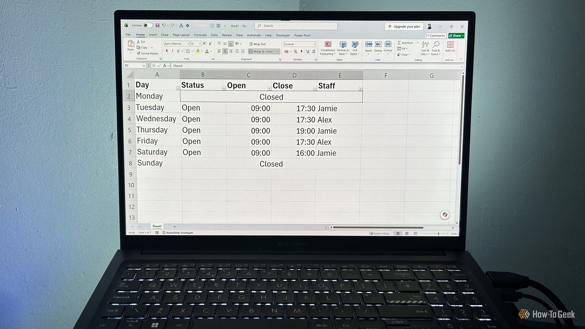
Ditch Merge & Center: The Better Way to Align Text in Excel
Learn to use Excel's "Center Across Selection" to align text across cells without merging, avoiding common data manipulation issues. This guide provides steps to utilize this newly accessible feature and add it to your Quick Access Toolbar.
Ars Technica's Rocket Report: Your Essential Space Industry Briefing
Quick Verdict Ars Technica's Rocket Report, presented by veteran space reporter Stephen Clark, offers an invaluable and meticulously organized weekly (or similar frequency, implied by "Edition 9.15") digest of the most
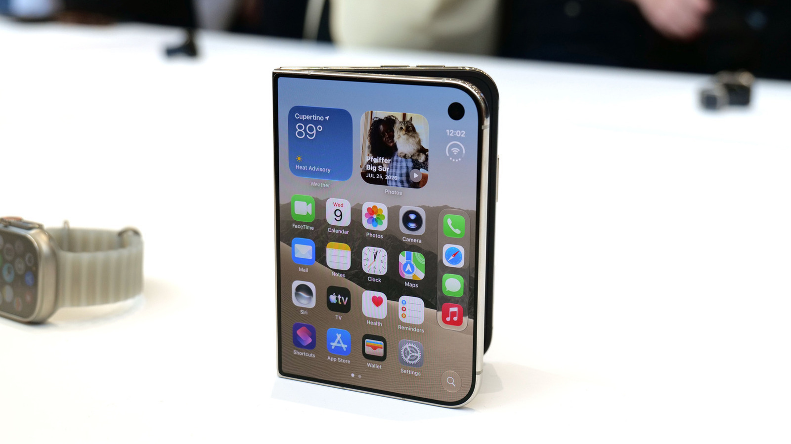
Apple iPhone Duo: A Daring Debut with Notable Compromises
Apple's highly anticipated iPhone Duo, priced at $2,000, has gone on pre-order. While hailed as "Apple's most exciting device in a decade" for its innovative foldable design and immersive display, it comes with significant drawbacks like the absence of FaceID and a premium camera.
Tesla Unveils Thruster-Equipped Roadster, 2028 Production Targeted
Tesla has unveiled its second-generation Roadster, featuring cold-gas thrusters co-developed with SpaceX, enabling it to jump and flip. The electric sports car demonstrated 0-60mph in an astonishing 0.81 seconds, with production targeted for 2028. This highly anticipated reveal also serves as a key recruitment tool for Tesla's ambitious AI and robotics initiatives.
AI's Confidence vs. Formal Methods' Rigor: Design Flaws & Verification
While AI accelerates code generation, formal methods remain critical for ensuring system correctness. Languages like TLA+ and tools like Quint enable developers to model and verify system designs before coding, catching subtle flaws. Quint makes formal methods more accessible with developer-friendly syntax and executability. This approach is vital for verifying AI-generated code through trace validation and model-based testing, ensuring reliability against real-world data.
KDE Plasma 6.8: A Future-Focused 30th Anniversary Update
Quick Verdict KDE Plasma 6.8, arriving as the "30th Anniversary Edition," is a pivotal release that decisively pushes the desktop environment into the future. With a definitive farewell to native X11 sessions and a