
IBM Sub-1nm Chip Technology: A Leap Forward, But Far Off
Quick Verdict IBM's latest sub-1 nanometer chip technology, featuring its innovative nanostack architecture, represents a significant breakthrough in semiconductor research. It promises unprecedented gains in compute
Quick Verdict
IBM's latest sub-1 nanometer chip technology, featuring its innovative nanostack architecture, represents a significant breakthrough in semiconductor research. It promises unprecedented gains in compute performance and energy efficiency, crucial for the future of AI and data centers. However, it's important to understand that the 'sub-1 nanometer' designation is a performance equivalent, not a literal physical dimension, and this foundational technology is still 5-10 years away from commercialization. While a monumental achievement in the lab, consumers won't see this directly in their devices anytime soon.
Redefining Chip Performance
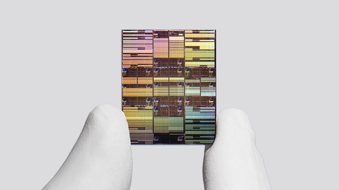
IBM has announced what it describes as the "world's first sub-1 nanometer chip technology," a development poised to nearly double transistor density compared to its previous generation of chips. This new architecture can integrate close to 100 billion transistors onto a chip the size of a human fingernail. The stated goal is to achieve substantial improvements in compute performance and energy efficiency, particularly for AI data centers, without a proportional increase in power consumption. According to Jay Gambetta, director of IBM Research, this isn't just a small step but a significant advancement pointing towards a future of much more powerful, yet energy-conscious, computing.
Decoding "Sub-1 Nanometer": Marketing vs. Reality
The "sub-1 nanometer" claim requires careful clarification. While the technology is branded at the 0.7-nanometer node (or 7 angstrom node), this number does not reflect the actual physical dimensions of the chip's features. For decades, chip node numbers have diverged from the literal size of transistors, especially as physical limitations make building functional components below 1 nanometer increasingly challenging. IBM’s claim signifies that its new nanostack architecture delivers the performance and density that would be expected from a hypothetical chip with sub-1 nanometer physical features, effectively pushing the boundaries of what's possible within existing physics.
The Nanostack Revolution: Engineering for the Future
At the core of this breakthrough is IBM's novel nanostack architecture, which builds upon their earlier work with nanosheet transistors. These nanosheets formed the basis of their 2-nanometer chip node, introduced in 2021. The nanostack innovation involves vertically stacking transistors in a staggered configuration, allowing for a much higher density of transistors within the same chip area. The basic unit comprises two transistors bonded and stacked together. Each individual transistor is made of three nanosheets, each approximately 5 nanometers thick (roughly 15 rows of silicon atoms), with a separation of about 9 nanometers between each nanosheet. This ingenious vertical integration is how IBM is overcoming the physical scaling limits that traditionally hinder chip design.
Performance Beyond Expectation: Fueling the AI Era
The projected benefits of the nanostack architecture are compelling. IBM's technical reports suggest that this technology could offer 50 percent higher computing performance or, alternatively, 70 percent greater energy efficiency compared to their previous 2-nanometer node chips. These figures highlight a critical advantage in an era increasingly dominated by demanding AI workloads. Furthermore, the nanostack architecture has shown a 40 percent improvement in scaling for static random-access memory (SRAM), which is vital for the fast read/write operations prevalent in many AI applications. This SRAM improvement is achieved through a staggered-channel design for SRAM bit cells, reducing their height by 40 percent and enabling more memory to be packed into the same chip footprint. This is significant, as SRAM scaling has seen only marginal improvements in recent chip generations, with only a few percent gain between 3nm and 2nm nodes, as noted by Jay Gambetta.
From Lab to Fab: The Path to Commercialization
IBM operates primarily as a chip technology research entity, not a commercial chip manufacturer. Its strategy involves partnering with leading semiconductor companies for mass production. Past collaborations include working with Japan's Rapidus for 2-nanometer chip production and Samsung for commercializing related technologies. IBM declined to name specific partners for the sub-1 nanometer technology, but Huiming Bu, vice president of IBM Semiconductors Global R&D, expects commercial chips incorporating this nanostack architecture to begin production within the next five to ten years. This timeframe suggests that while the technology is groundbreaking, it's a long-term investment that will shape the industry for decades, potentially replacing nanosheet architectures as the mainstream in CPUs and GPUs.
Pros and Cons of IBM's Nanostack Technology
Pros:
- Significant Performance & Efficiency Gains: Projected 50% higher compute performance or 70% greater energy efficiency, critical for future demanding applications like AI.
- Innovative Architecture: The nanostack design, with vertically stacked transistors and improved SRAM scaling, pushes the boundaries of semiconductor engineering.
- Future-Proofing AI Workloads: Enhanced SRAM scaling and overall compute power are vital for supporting increasingly complex AI and data center operations.
- Pioneering Research: IBM continues to demonstrate leadership in foundational chip technology research, setting industry standards for future manufacturing.
- Potential for Widespread Adoption: Nanosheet technology, previously pioneered by IBM, has become mainstream for 2nm and 3nm chips, indicating a strong likelihood of this new tech following suit.
Cons:
- Long Commercialization Timeline: It will take 5-10 years before chips based on this technology enter mass production, meaning immediate consumer impact is zero.
- "Sub-1 Nanometer" is a Marketing Term: The node number does not reflect actual physical feature sizes, which can be misleading for those unfamiliar with current semiconductor nomenclature.
- Not a Direct Consumer Product: IBM focuses on research and licensing; actual end-user products incorporating this technology will depend on manufacturing partners like TSMC or Samsung.
- Dependence on Partnerships: Commercial success hinges on successful collaboration and adoption by major foundries, which is not guaranteed.
The Competitive Landscape: IBM's Pioneering Role
In the current semiconductor landscape, companies like TSMC and Samsung Foundry are at the forefront of advanced chip manufacturing. The source content highlights that IBM's previous nanosheet transistor architecture paved the way for its 2-nanometer chip node, and that nanosheet technology is now widely adopted by leading foundries, including TSMC for its proprietary 2-nanometer node. This demonstrates IBM's historical role as an innovator whose research often becomes the foundation for the next generation of commercial chips. Therefore, a direct comparison table for IBM's sub-1 nanometer technology against commercial products from TSMC or Samsung isn't appropriate or feasible at this stage. IBM is claiming to be the first with this particular technology. The competitive context is that IBM is once again pushing the envelope, setting a new benchmark that other foundries will likely work to adopt and commercialize in the coming years, much as they did with nanosheet technology.
Recommendation: Investing in Tomorrow's Compute
IBM's sub-1 nanometer chip technology is not a product you can buy today, nor is it likely to be one in the next several years. For industry analysts, investors in semiconductor manufacturing, and companies heavily reliant on high-performance, energy-efficient computing (especially for AI), this announcement is incredibly significant. It signals the continued exponential growth of computing power and efficiency, offering a glimpse into the next decade of technological advancement. For the average consumer, this is a 'watch this space' development. While its direct impact is distant, it promises to power the faster, smarter, and more efficient devices and services of tomorrow. IBM continues to be a crucial force in fundamental semiconductor innovation, and this latest announcement reinforces its role as a trailblazer.
FAQ
Q: What does "sub-1 nanometer" actually mean for this chip technology?
A: It means the chip's architecture, called nanostack, achieves performance and density equivalent to what would be expected from a theoretical chip with physical features smaller than 1 nanometer. It does not mean the individual physical components on the chip are literally smaller than 1 nanometer; node numbers are primarily marketing and performance indicators in modern chip manufacturing.
Q: When can I expect to see devices powered by this IBM technology?
A: IBM states that commercial chips incorporating this sub-1 nanometer technology could begin mass production within the next five to ten years. Therefore, it will be quite some time before this innovation translates into consumer products or even widely available data center hardware.
Q: How does this technology improve AI performance?
A: The nanostack architecture offers significant gains in raw compute performance and energy efficiency. Crucially, it also provides a 40 percent improvement in SRAM scaling, which is vital for the fast, on-chip memory access required by intensive AI workloads, leading to faster processing and lower power consumption for AI applications.
Related articles
Android 17 QPR2 Beta 7.1: The Performance Relief You've Been Waiting
Android 17 QPR2 Beta 7.1: Finally Fixing the QPR1 Performance Woes Verdict: Android 17 QPR2 Beta 7.1 is a crucial and highly anticipated software update for Google Pixel users, specifically targeting and resolving the

DJI Solo Video Setups: Smart Choices for Lone Creators
This review delves into DJI's recommended solo video setups, highlighting the Osmo Pocket 3 Creator Combo as a top pick for its integrated camera, gimbal, and mic. It also covers stabilizers like the Osmo Mobile 8 and RS 4, and the DJI Mic Mini series for enhanced audio, providing honest pros, cons, and clear buying advice.

Ars Technica's Rocket Report: Your Essential Space Industry Briefing
Quick Verdict Ars Technica's Rocket Report, presented by veteran space reporter Stephen Clark, offers an invaluable and meticulously organized weekly (or similar frequency, implied by "Edition 9.15") digest of the most

Apple iPhone Duo: A Daring Debut with Notable Compromises
Apple's highly anticipated iPhone Duo, priced at $2,000, has gone on pre-order. While hailed as "Apple's most exciting device in a decade" for its innovative foldable design and immersive display, it comes with significant drawbacks like the absence of FaceID and a premium camera.

AI's Confidence vs. Formal Methods' Rigor: Design Flaws & Verification
While AI accelerates code generation, formal methods remain critical for ensuring system correctness. Languages like TLA+ and tools like Quint enable developers to model and verify system designs before coding, catching subtle flaws. Quint makes formal methods more accessible with developer-friendly syntax and executability. This approach is vital for verifying AI-generated code through trace validation and model-based testing, ensuring reliability against real-world data.

Amazon Prime Video Launches AI-Powered Prime 360 for NBA Coverage
Amazon Prime Video is elevating its NBA coverage with the introduction of Prime 360, an AI-powered replay system offering immersive, 'fly through' views of the action. Kicking off its second season, Prime Video also adds Yahoo fantasy integration and gains exclusive Eastern Conference Finals rights, expanding its tech-driven sports broadcast. The new features aim to deliver a unique and interactive viewing experience for basketball fans.